After extracting the calculator's firmware from the updater in Part 1, we can get finally down to details and see what this device can actually do. If you're interested in Windows reversing and haven't read Part 1 already, check it out!
After extracting the firmware images, we're left with two binary files that don't have much meaning yet. They're full of compiled machine code, and we've got to disassemble the files to make any sense of them. Our first step in disassembling the files is to identify the processor, so our decompiler (IDA) knows how to turn our binary files into readable assembly.
We'll only be dealing with the 3070 firmware image throughout this post, as it's the main software for the calculator. I'm also not too enthusiastic about bricking my calculator, which could be easy to do if I messed around with the bootloader firmware (3069) too much.
Identifying the processor
When I first started this project, this took me longer than I care to admit. Looking at pictures of the calculator's PCB shows no identifying marks - the main CPU is a epoxy-covered COB (chip on board) with no etchings or other markings. Unsurprisingly, the CASIO website gives no information in this regard, and simply searching "fx-CP400 processor" on Google brings up no useful hits.
Searching the web now, I can easily find many resources that point to the Renesas SuperH (specifically, SH4) architecture used by the calculator [1] [2]. Since I'm not sure how I originally discovered the calculator used an SH4 processor, I'll just speculate on how I may have. Luckily, the fx-CP400 has many similar models and a well-documented predecessor, the ClassPad 330. This device is known to use a SH3 processor. I may have used this information to start searching for "fx-CP400 SuperH" and found one of the pages I linked above. This is a good strategy if you're completely unsure about the processor of the device you're handling - find older predecessors that may be better documented, or very similar products. They can give you a starting point that may lead you to wealths of helpful information.
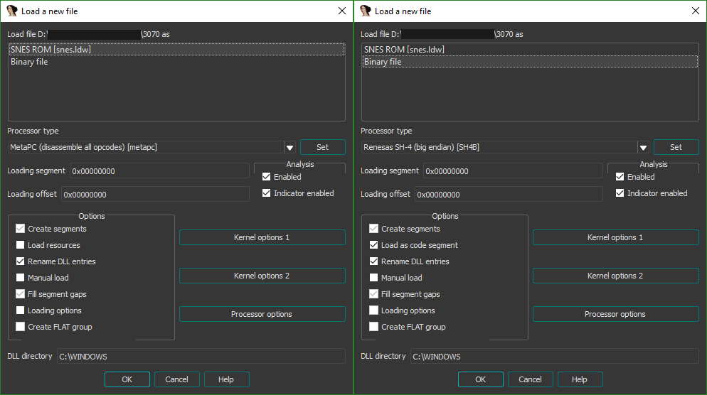
Now that we know the processor type, we can start loading our binary into IDA. It initially tries to tell us our file is a SNES ROM running on a MetaPC (left), but we correct it by loading as a binary file and setting the processor type to the Renesas SH4 (right).
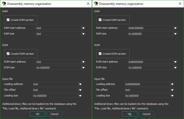
Now, IDA asks us about the memory regions we want to set up. Since we're loading a simple binary file, IDA doesn't know where the data we're giving it ends up in memory. When you open a compiled ELF or PE file, a header inside the file gives the operating system and decompiler information about where each section of the file should be loaded in memory. Since all we've got is a binary blob that's dumped directly into the calculator's ROM, we've got to manually tell IDA where it all goes.
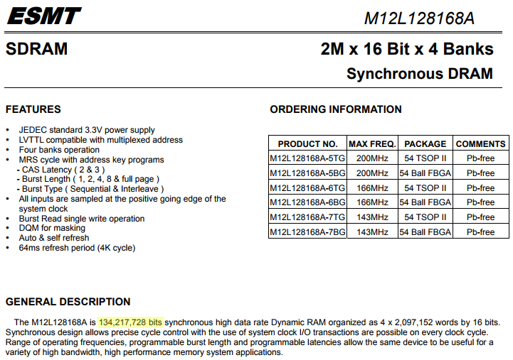
Identifying the length of our RAM section isn't too hard - referring to the forum post found in Part 1, we know the RAM IC in the calculator is an M12L128168A. Searching for the part's datasheet, we find it can hold 134,217,728 bits, or 0x1000000 bytes. We don't know the length of the ROM for sure yet, but it's safe enough to just use the length of the firmware file we have. Since the NAND flash is also used for the calculator's FAT filesystem and MCS, the ROM will certainly be larger than 0x1500000 bytes, but that won't matter for now. More research reveals RAM likely starts at 0x8C000000, and even more research shows ROM likely starts at 0x80000000.
Even if we got these addresses slightly wrong, we'd find out quickly enough. When IDA attempts to mercilessly cross-reference our binary, any issues would become obvious. So, let's set up our memory.
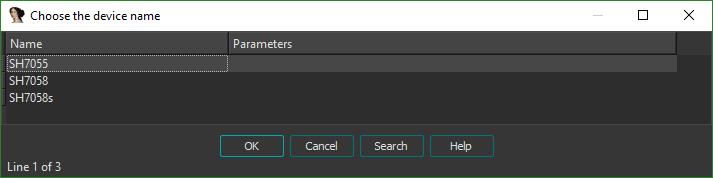
IDA then asks us to choose exactly which SH4 device the code we're disassembling is for. Problem is: our specific SH4 processor is a custom model made for CASIO, that's not publicly documented at all. We're lucky, however, that these options basically only affect the labels IDA places on some memory addresses representing MSRs (model specific registers) to identify them. We'll just pick the first one and start the disassembly.
Exploring the firmware
Now comes the time we've got to discuss the SuperH architecture used by the fx-CP400. There are a few quirks which, unless you've worked with SuperH before, won't be obvious at all. There are 16 general purpose registers, r0 to r15. Registers r0 to r7 are not required to be preserved through function calls, but r8 to r15 are. The register r15 is used as the stack pointer. The calling convention used is quite simple - arguments are passed in registers r4 to r7 and then on the stack if registers run out. Return values are passed back in the r0 register.
The processor also makes use of what's known as a delay slot. After most branches, the instruction directly following the branch instruction is executed before the branch is or isn't taken. Take the following two pieces of assembly for example.
# 1
mov #1, r4
mov #2, r5
call my_function
mov #3, r6

# 2
bt my_label # conditional jump
mov #1, r4
my_label:
mov #2, r5
In the first code sample, the instruction moving 3 into r6 will be run before the call. In my_function, the value of r6 would be 3. In the second code sample, the mov #1, r4 instruction will be run, no matter the outcome of the conditional branch. No matter if the jump is or isn't taken, the delay slot instruction will be run. Keep this in mind - it's a gotcha that can make a simple function seem a lot more confusing than it actually is. With that out of the way, let's finally look at the firmware.
Considering the complexity of the device we've got in our hands, starting our investigation at the very start of the firmware image isn't the best idea. It's likely that there'll be enough complicated setup and initialization (the LCD, the keypad, the flash, etc.) that we could very easily get lost and never actually reach anything interesting. So to begin, let's start with a place in the code we know will exist. In Part 1, we quickly discussed the debugging menu reachable by holding [=] and [EXP] and turning the GC on. Mashing [LEFT] and [z] brings us to a selection menu.
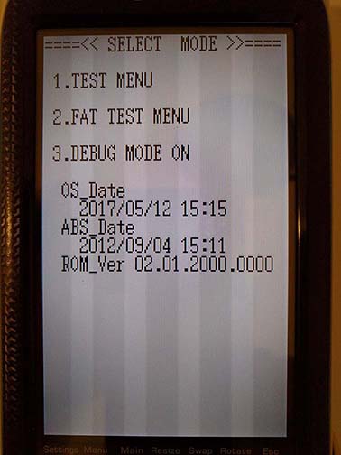
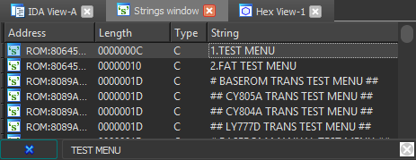
We'll use the strings we see in the the debug selection menu to break into the firmware. The goal here is to discover how the menu is drawn to the screen, and hopefully write our own text onto the display at some point. We'll open the Strings window in IDA, and search for the string TEST MENU, from the first menu option on the mode selection screen. We're presented with a ton of strings, but the first result matches the menu item exactly. Double clicking the string in the window takes us to the location it's stored in the firmware, and checking the cross references shows two locations the string is referenced.
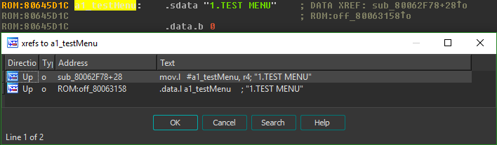
The first reference we see (in a mov instruction) is the true use of the string. The second reference (in a .data.l directive) is storing the address of the string in a constant pool after the function it's used in. Since instructions on the SH4 platform are constant length, it's not possible to store a whole address within the instruction and instead the full value must be placed in another memory location within reach of the instruction. Thankfully, IDA makes the usage of a constant pool transparent to us, and simply shows the mov instruction moving the address of the string into the r4 register.
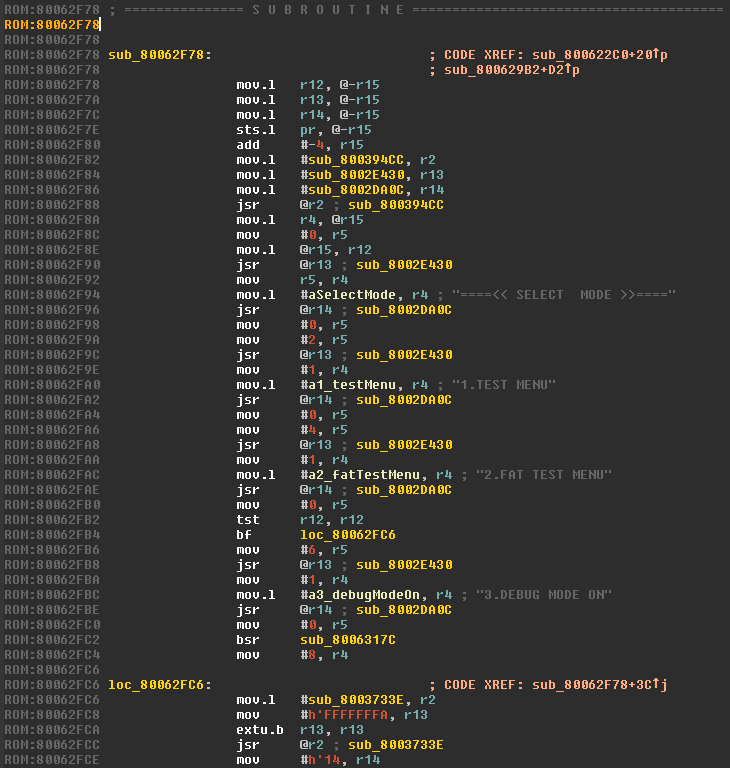
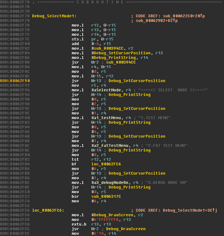
To make our lives easier later on, we'll name the function we're looking at something that'll help us keep track of it. For these functions used in the debug menus, I've utilized the prefix Debug_ to differentiate them from those in the main OS. I've called this function Debug_SelectMode1 (because I know there's a second screen with SELECT MODE on it!).
Luckily for us, there are multiple strings printed here. This makes it a lot easier to confirm that the functions we find actually do what we think they do. Looking at how each string is used, we see that the string's address is loaded into r4 and then the function address stored in r14 is called (jsr jumps to a subroutine, jsr @r14 jumps to a subroutine whose address is in r14). In the delay slot, the value 0 is placed into r5. This shows us there's probably only two arguments to the function - the string and an unknown second argument. Since it clearly prints the string it's given, we'll rename the function loaded into r14 from sub_8002DA0C to Debug_PrintString.
Interleaved throughout the Debug_PrintString calls, is a call to another function sub_8002E430. If we examine the arguments passed in to the function, we start to notice a pattern.
r4 = 0      r5 = 0
r4 = 1      r5 = 2
r4 = 1      r5 = 4
r4 = 1      r5 = 6
Before the first string is printed, the function is called with the arguments 0 and 0. As the next three strings are printed, the first argument is always 1 whilst the second argument increases by 2. Looking back at the debug screen, we notice each of the menu options is displayed with a one line gap between each. Counting characters, we notice the arguments to the function coincide with the position the string is printed. We've discovered the function used to set the position of the cursor, so let's call it Debug_SetCursorPosition.
We've now identified almost all the functions used in this small section of code. There's one function we haven't found, whose existence isn't necessarily obvious. This is a function which displays the changes we've made to the screen, equivalent to a swapping buffers in a more sophisticated graphical application. There are two function calls which immediately follow our cursor position setting and string printing functions.
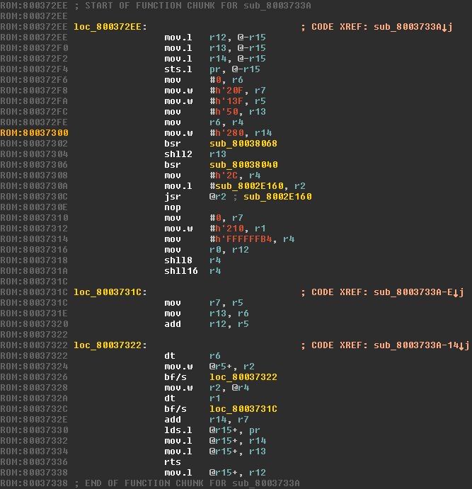
Inspecting the first function, sub_8006317, shows it makes many calls to the Debug_PrintString function with some strings we can recognize from the debug menu. It's unlikely this is our drawing function. The next function (sub_8003733E), however, calls directly to another function which calls another function. After traversing the maze, we're shown a function (loc_800372EE) which looks quite unremarkable. This is likely our screen drawing function. To confirm, we can look at other locations where the Debug_PrintString function is used, and check if our newly identified function is used there as well.
Since we're now pretty sure sub_8003733E is our screen drawing function, we'll rename it to Debug_DrawScreen. Our initial section of code, Debug_SelectMode1 now looks like this.
Let's write a short snippet of code to test the functions we've discovered. This is the step we're going to need our SH4 cross-compiler for. If you'd like to know how to build a cross-compiler for SH4 yourself, check out Part 2.1.
Since they're annoying to deal with, we'll place nop instructions in every delay slot to avoid them. This is a Gist with the assembly code we've written to test these functions. It's thoroughly commented, so even if you're not familiar with SH4 assembler you'll probably understand it.
We'll save this file as main.s and compile the code into a flat binary, ready to be copied into some location within the firmware.
sh4-elf-as main.s -o main.o
sh4-elf-objcopy -O binary main.o main.bin
The file main.bin is then ready to be inserted into the firmware. The location where we do this is important to determine. We can't just paste it at the first address in the firmware, as we'd overwrite vital initialization code and could possibly even brick the device. We've got to find a location where we can control execution, i.e a piece of code we can trigger when we want. We find that we can make a "Check" button appear within the language selection dialog in the System app, when the debug mode is enabled. This debug mode can be triggered through the debug menu.
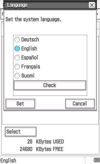
We'll do a search for one of the strings that appears within the Check menu and place our code there. This location ends up being 0x80133144, which is the location 0x133144 within our firmware image. Since our code will halt once it's finished, we don't have to worry about returning from the function we're overwriting. We open the 3070 firmware file with a hex editor, and copy the bytes from our generated main.bin file into the firmware file at the address 0x133144. We must ensure we're overwriting the bytes within the firmware file, rather than inserting our code and displacing the bytes that follow.
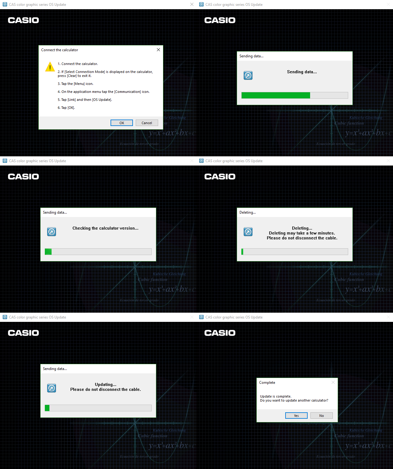
Using a short Python script, we compress the firmware file in the same way as seen in the OSupdateDLL.dll file. Taking care to ensure the missing byte reported by the tool is the same as the one which is hardcoded into the DLL, we embed it back into the DLL file using a resource editor.
With the modified OSupdateDLL.dll and original fxASPI.dll and LanguageResource.dll files in one directory, we can run the updater. Running the command rundll32 OSUpdateDLL.dll,OSUpdate launches the firmware updater and we're almost ready to flash. Since the version of firmware we're attempting to write into the calculator is the same as the one which is running on it, simply using the OS Update menu option within the Communication app won't work. We must launch the calculator into emergency OS update mode by holding down [EXP], [^] and [Clear] while pressing the reset button on the back of the calculator. We can then plug the calculator into the computer and run the update.
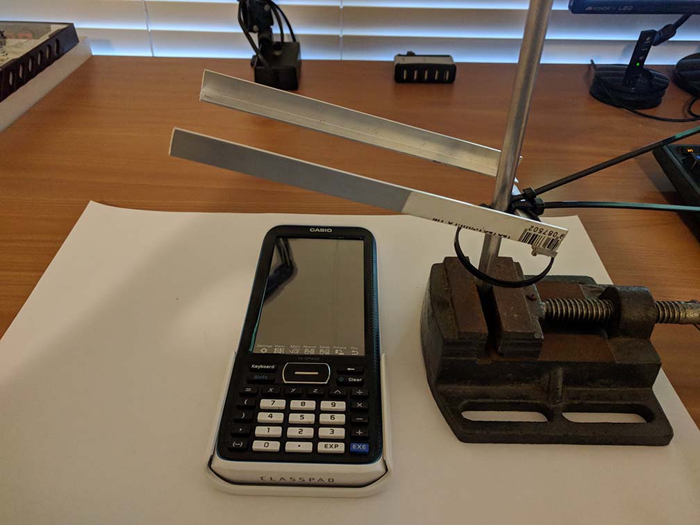
We've now managed to load our own code onto the fx-CP400 and..... it works! At least the software does, the video - not anywhere near as well.
Concluding note: I managed to spill probably 25 mL of water over the graphics calculator while writing this post. Luckily it was mostly confined to the keypad section, but some water did manage to splash onto the screen. After a thorough disassembly and drying, the GC seems to have survived.
The lesson is simple - don't leave partially full glasses of water on your desk when you're constantly reaching around. It's a really bad idea.
If you're also interested how I recorded that video.... check out this image if you want to see some great amateur metal work.