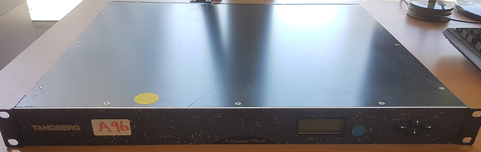
This is the Tandberg (now owned by Ericsson) TT6120 TS Processor. Catchy name, I know. I picked it up at a hamfest recently, out of sheer interest regarding what it was and what was inside it.
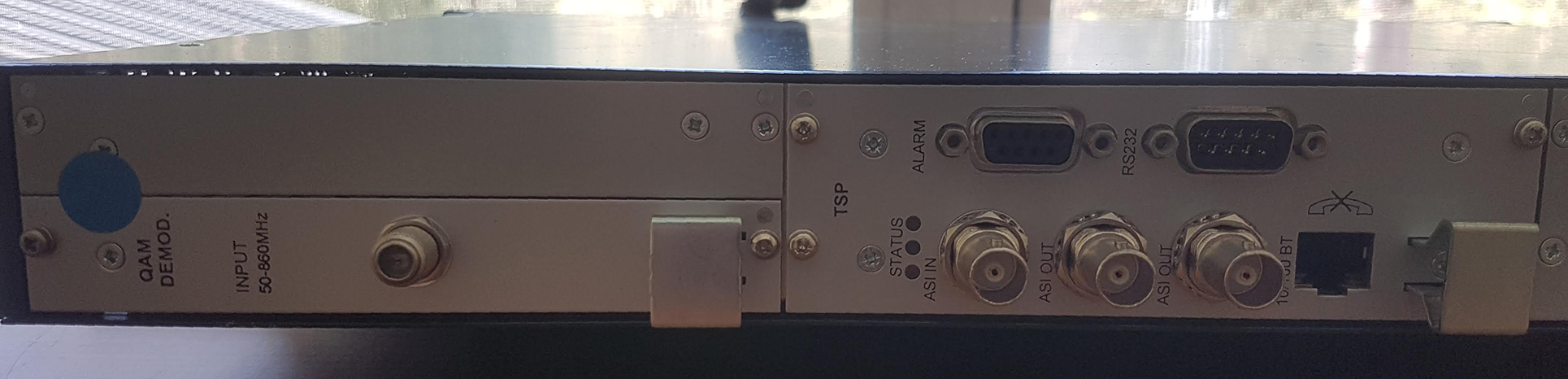
With a bit of Googling (and the help of an expert) I found out it's a "transport stream processor" - a device which takes in one source of video, and spits out another (possibly in a different format). In the device I picked up, a QAM (an RF modulation method) demodulator acts as one input, and an ASI (a serial video format) interface as the output.
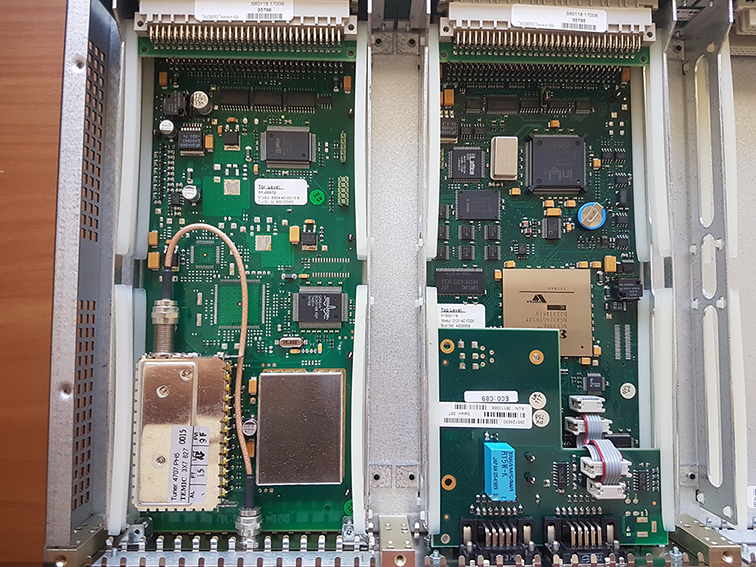
It's quite a pretty device once you pop the lid off. The modular structure of the device hinted to by the handles and bolts on the rear of the device is confirmed - both blocks connect to a backplane with common connectors. Since many other input and output formats are supported by the device, it's a much cheaper solution than having to spin many different boards for each combination of input and output format.
Pictured below is the QAM demod (left) and TSP (right) modules.
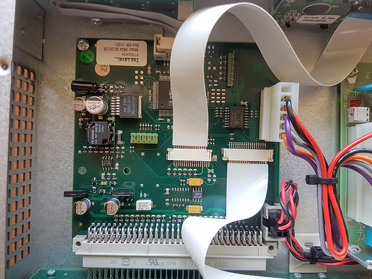
The backplane connects to this small common board, which only has a single Lattice PLD, some power supply components and acts as an interface between the front panel LCD and buttons and the backplane.
RF
The QAM demodulator module is intended to receive a DVB-C cable TV signal and extract the video data from it. The module has a tuner capable of receiving from 50 MHz to 860 MHz (producing an IF of 36.125 MHz), which is then fed into another mixer to bring this 1st IF to the 44 MHz 2nd IF frequency required by the QAM demodulator IC.
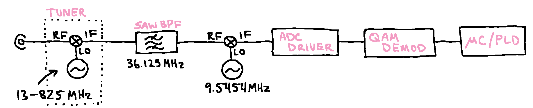
Note: there's definitely something weird with this I don't understand. The LO of the dedicated mixer is a 28.636363 MHz crystal - but adding/subtracting ~28 MHz from the 36.125 MHz IF from the tuner gets you nowhere near the IF of the QAM demodulator IC - 44 MHz. However, 1/4 (or 1/3) of the crystal's frequency gets much closer to the demodulator's IF, though I know that doesn't make much sense (it's the closest I can get to understanding this though!). I'm not an RF expert so please, please - if you know how this is meant to work, do tell!
Embedded
JTAG
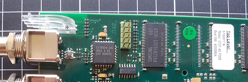
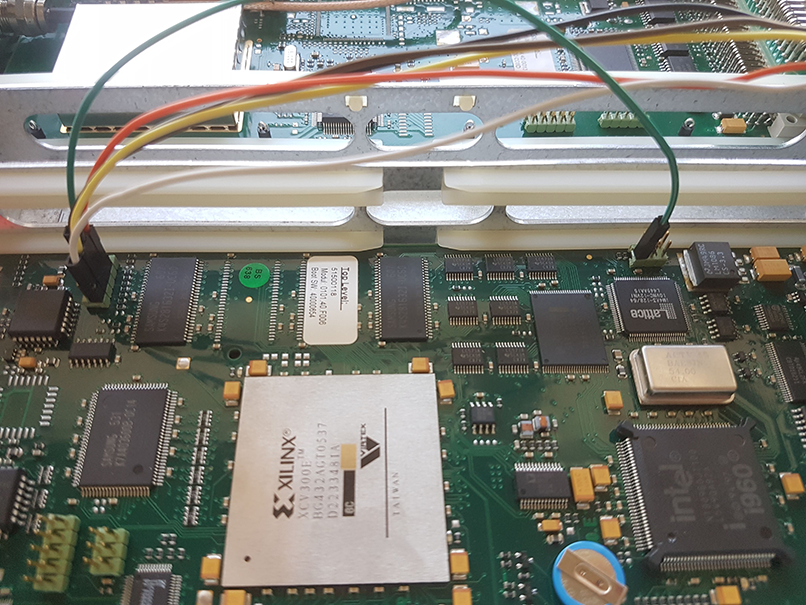
Most of the processing power in the device is housed in the TSP module. On the board is a large Xilinx XCV300E FPGA and an Intel i960 embedded processor. Interestingly, under the serial port/alarm connector PCB, there's a lovely connector labelled "JTAG". With a bit of probing, it's not too hard to find the pinout of the connector.
Identifying the GND pin is the easiest - check for continuity between the GND pin on basically any of the digital logic ICs and each of the pins on the JTAG header. Turns out it's pin 8 (numbering from pin 1, right-to-left, bottom-to-top in the perspective of the picture).
Now, the JTAG signals of TCK, TMS, TDI and TDO can be found. TCK and TMS shouldn't be too hard - they're shared between every TAP in the scan chain, but TDI and TDO are chained through each device. Annoyingly, checking for continuity between the TCK pin on the i960 and each pin of the header gave no results. No pin of the header appeared to connect to the TCK pin of any of the 3 devices in the scan chain (Xilinx FPGA, Lattice PLD and the Intel i960) - and neither did the TMS pin.
Testing the visible components around the JTAG header showed that most pins connected through a resistor to the small SOP-16 package IC below it. A single Google search later showed the part was a SN74LVTH125 bus buffer - but why's it there? As it turns out, each of the devices in the chain run on a 3V3 VCC, but the manufacturer clearly desired/only had hardware that would support a 5V JTAG interface. As such, the bus buffer acts as a level converter between the 3V3 logic on the board and the 5V signals of a JTAG adapter.

Now, it was clear that all four of the JTAG signals would pass through the bus buffer before making their way to the devices on the chain. Quickly the TCK and TMS pins were found to be 1 and 3 (respectively). Now comes identifying the TDO and TDI lines. Probing the TDO and TDI pins of the i960 showed no connection to the bus buffer, so it's clear it's in the middle of the scan chain. The TDO pin of the i960 did connect to the TDI pin of the Lattice iM4A PLD however, and tracing the PLD's TDI showed it eventually making connection to pin 5 of the JTAG header.
Since it was now clear that the Xilinx FPGA was the first device in the scan chain, finding the TDO pin would be harder than the rest. As a big BGA device, there's no easy (and non-destructive) way to access the balls of the device, so simple continuity checking to find the pin was out of the question. Luckily, the pattern formed by the pins on the header seemed clear - TDI should logically appear on pin 7.
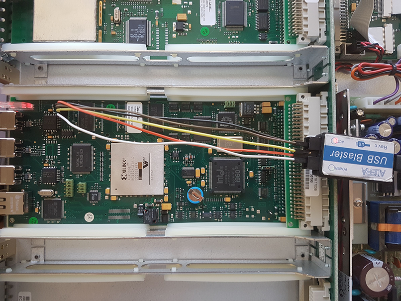
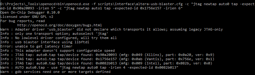
So I connected my JTAG adapter (read: Altera USB Blaster clone), plugged the Tandberg in, and crossed my fingers.
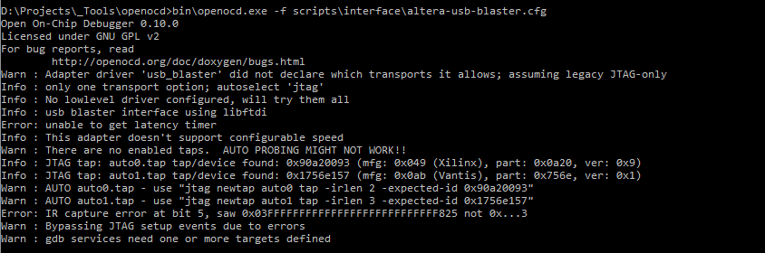
Hrm. Only two devices - the FPGA and PLD. Where's the i960?
Darting to the i960's datasheet, the TRST# pin is immediately a possible culprit. When it's held low, the JTAG debug interface is disabled and is only enabled when the pin is high. A quick check with the multimeter shows the pin is always in a low state. Hmm.
Tracing the pin's path on the PCB, again simply with my multimeter's continuity test, showed the pin driven by an output of the bus buffer with a pull-down resistor to ground. Easy - just drive the input to the buffer low (inverted output - driving the input low results in a high output) and the JTAG port will be enabled. Just one spanner in the works though: the input to the buffer is directly connected to VCC, so there's no way it can be pulled low. The input doesn't even appear on a pin on the JTAG connector.
After a bit of head scratching (and random, uncoordinated continuity checking), I discovered the output enable pin (!) of the particular buffer outputting to the TRST# line was connected to the JTAG header. Pulled high with a 100 ohm resistor, it's as simple as pulling the OE line (pin 10 on the header) to ground.
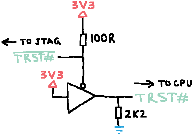
A link between the pin and a GND on another header later, and the full scan chain appears in all its glory.
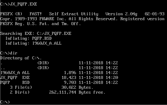
Sadly though, with the age of the parts, the processor appears to only implement boundary scan and the PLD and FPGA are "sparse" in regards to the amount of information about them on the internet. A great sign of their age is the BFDL for the i960, which came in a self extracting EXE: not a Windows executable, but a DOS one. DOSBox to the rescue.
Serial
On the rear of the device, there's an RS-232 port which is "for service personnel only" according to the manual. I fancy myself as a bit of a service personnel anyway, so I thought I'd dig in.
Thanks to the joyous non-standard nature of RS-232 serial ports, this took more effort than it needed to. Connecting to the serial port with the only female-female serial cable I could find gave no results, no matter the baud rate. Checking the TX line of the port on the scope showed some data bursts, but the USB-Serial adapter refused to communicate. Most likely an issue with either the port on the Tandberg or the cable I was using being wrong (i.e. the RX/TX flipped on the Tandberg, or my serial cable being something other than a null-modem cable), the next step was to try and swap the TX and RX lines to see if any data would appear.
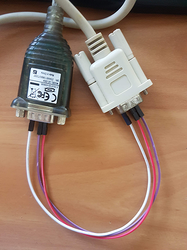
After building my poor-man's null-modem cable and fiddling with the baud rates, data finally poured through.
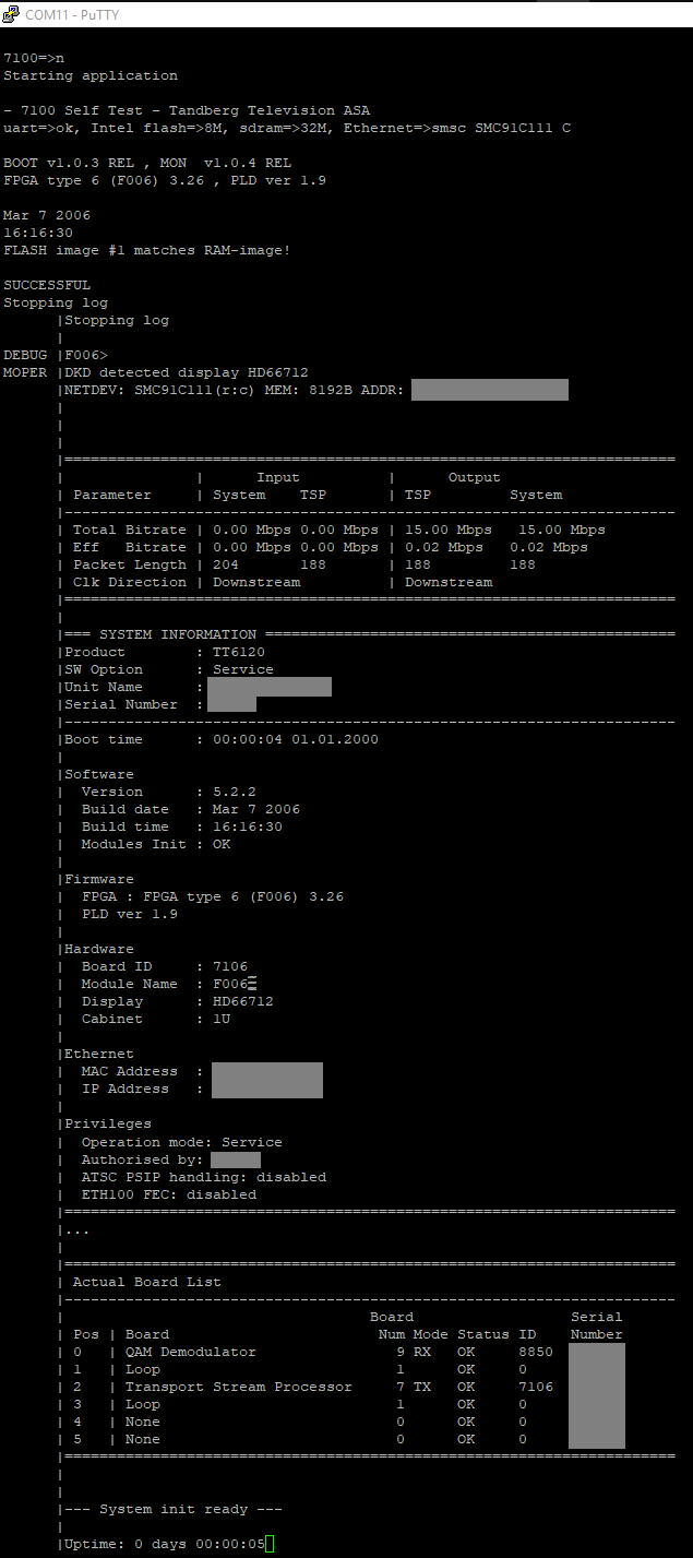
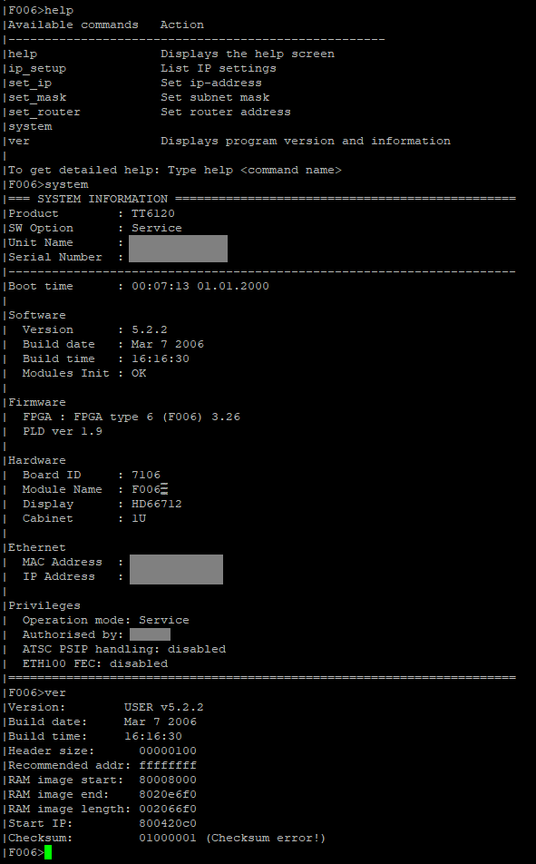
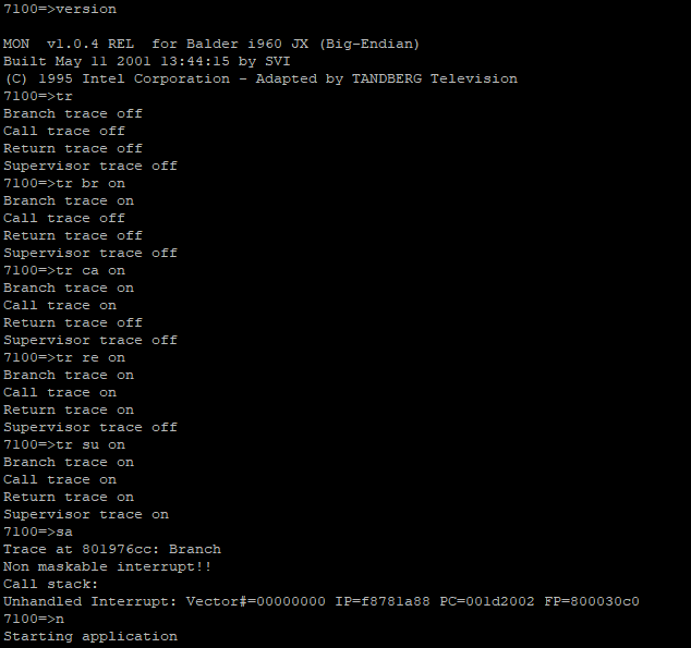
Mashing Enter brings us to a command line, with a couple interesting commands. system gives us the information we've already seen at boot, but ver gives us some stuff we haven't yet seen.
I kinda hoped there'd be a more interesting debug interface, so I started typing random commands until...
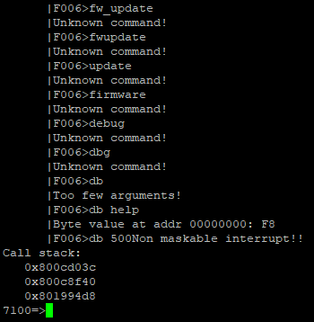
Interesting! db seems to read from memory somewhere, but given the address 500 (or any over 400 as it seems), causes an NMI that dumps us to a completely different prompt. What if we run help from here?
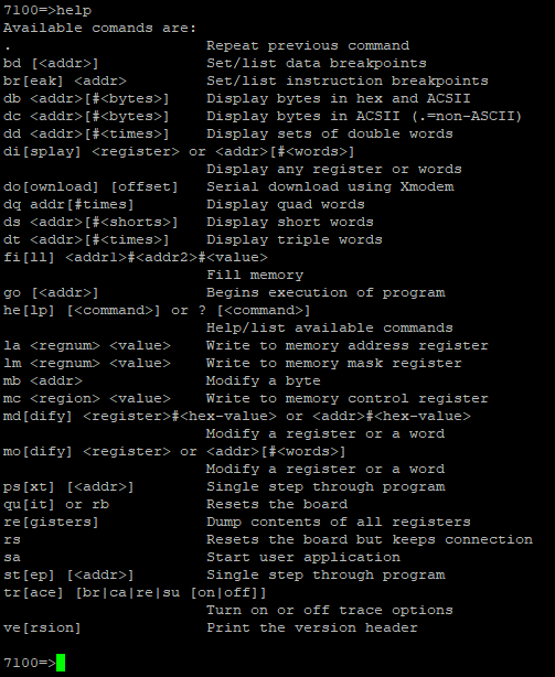
Of course, I couldn't resist running half of these commands.
Sadly, it seems pretty trigger-happy when it comes to firing random NMIs. I tried to dump the firmware using the di command (both as one big block and as multiple blocks of ~256 bytes) but both approaches cause it to lock up part way through.
Summary
That's about it. It's an interesting box, and I can only imagine the shocking cost for each of these parts individually in this device's heyday - let alone how much it cost to buy new and the service contracts associated with it. Though I'm sure it served its owners well,
If you've got any ideas on what to do with it (apart from throw it away 😂) I'd love to hear. The tuner is pretty cool - downconverting anything from 50 to 860 MHz down to around 30 MHz. Might be able to do something SDR-y with it? Trying to mess around with the FPGA and PLDs is probably a lost cause since I can't reverse engineer the bitstreams (let alone retrieve them from the devices anyway).
Hope this was an interesting read.